

Features
- Molded epoxy body
- FCC Part 68

File No.:E75887

Ordering Information
| D | 1A | 05 | D – | XXXX |
|---|---|---|---|---|
| Model | Contact Arrangement | Coil Voltage | D:With Diodes Blank:Without the Diodes | Customer code |
| S | 1A | 05 | D – | XXXX |
|---|---|---|---|---|
| Model | Contact Arrangement | Coil Voltage | D:With Diodes S:Metal Cover | Customer code |
Coil Data at 25°C
DIP Specifications
| Contact Form | Part Number | Nominal Voltage (VDC) | Coil Resistanece ±10% | Must Operate (VDC) | Must Release (VDC) | Rated Current (mA) | Continuous Voltage (max) | Circuit Schematic |
|---|---|---|---|---|---|---|---|---|
| 1A SPST-NO | D1A05(D) | 5 | 500 | 3.75 | 1.0 | 10 | 10 |  |
| D1A12(D) | 12 | 1000 | 9.00 | 1.2 | 12 | 20 | ||
| D1A24(D) | 24 | 2150 | 18.00 | 2.4 | 11.1 | 28 | ||
| 1B SPST-NC | D1B05(D) | 5 | 500 | 3.75 | 1.0 | 10 | 7 | 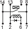 |
| D1B12(D) | 12 | 1000 | 9.00 | 1.2 | 12 | 15 | ||
| D1B24(D) | 24 | 2150 | 18.00 | 2.4 | 11.1 | 28 | ||
| 2A DPST-NO | D2A05(D) | 5 | 140 | 3.75 | 1.0 | 35.7 | 10 | 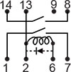 |
| D2A12(D) | 12 | 500 | 9.00 | 1.2 | 24 | 20 | ||
| D2A24(D) | 24 | 2150 | 18.00 | 2.4 | 11.1 | 28 | ||
| 1C SPDT-CO | D1C05(D) | 5 | 200 | 3.75 | 1.0 | 25 | 10 |  |
| D1C12(D) | 12 | 500 | 9.00 | 1.2 | 24 | 20 | ||
| D1C24(D) | 24 | 2150 | 18.00 | 2.4 | 11.1 | 28 |
SIP Specifications
| Contact Form | Part Number | Nominal Voltage (VDC) | Coil Resistanece ±10% | Must Operate (VDC) | Must Release (VDC) | Rated Current (mA) | Continuous Voltage (max) | Circuit Schematic |
|---|---|---|---|---|---|---|---|---|
| 1A SPST-NO | S1A05(D) | 5 | 500 | 3.75 | 1.0 | 10 | 10 |  |
| S1A12(D) | 12 | 1000 | 9.00 | 1.2 | 12 | 20 | ||
| S1A24(D) | 24 | 2000 | 18.00 | 2.4 | 12 | 28 |
*Form B SIP Available
CHARACTERISTICS
| Item \ Contact Form | 2A,1A,1B | 1C |
|---|---|---|
| Contact Resistance | 100mΩ max. (Initial) | 150mΩ max. (Initial) |
| Operate Time(Max.) | 0.5ms | 1.0ms |
| Bounce Time(Max.) | 0.5ms | 2.0ms |
| Release Time(Max.) | 0.2ms | 0.2ms |
| Insulation Resistance(Min.) | 1011Ω | 1011Ω |
| Contact Material | Precious Metals | Precious Metals |
| Power(Max.) | 10VA | 3VA |
| Switching Voltage(Max.) | 200VDC | 100VDC |
| Switching Current(Max.) | 0.5A | 0.25A |
| Carry Current(Max.) | 1.0A | 0.5A |
| Life Expectancy | 108 (Signal level) | 5×10⁷ (Signal level) |
| Breakdown Voltage | DC250V across open contact | DC200V across open contact |
| DC500V between coil and contact | DC500V between coil and contact | |
| Storage Condition | -40°C ~ +85°C | -40°C ~ +85°C |
| Operating Condition | -40°C ~ +70°C | -40°C ~ +70°C |
| UL Class B/F | Insulation System Class B/F | Insulation System Class B/F |
| Minimum Permissible Load | 100mVDC 10μA | 100mVDC 10μA |
| Vibration | 20g(10 ~ 2000Hz) | 20g(10 ~ 2000Hz) |
| Resonant Frequency | 3.5 KHz | 3.5 KHz |
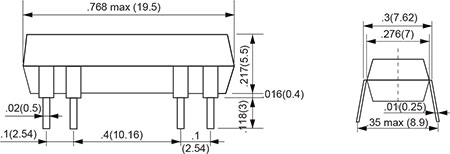
OUTLINE DIMENSIONS Unit: inch(mm)
DIP Type
SIP Type

Remark:
1) In case of no tolerance shown in outline dimension: outline dimension ≤1mm,tolerance should be ±0.2mm; outline dimension >1mm and ≤5mm,tolerance should be ±0.3mm;outline dimension >5mm, tolerance should be ±0.4mm.
2) The tolerance without indicating for PCB layout is always ±0.1mm.
PACKAGING SPECIFICATION
| TUBE | OUTER CARTON | OUTER CARTON SIZE |
|---|---|---|
| 25PCS | 5000PCS | L540mm*W200mm*H165mm |
APPLICATION GUIDELINES
Automatic Wave Soldering
* Wave solder is the optimum method for soldering.
* Adjust the level of solder so that it does not overflow onto the top of the PC board.
* Unless otherwise specified, solder under the following conditions depending on the type of relay.
| Preheat time 20°C-100°C | Rising slope 20°C-120°C | Decreasing slope Peak-150°C | Slodering temperature 255°C-265°C |
|---|---|---|---|
| 90±5 seconds | <3°C/s | <4°C/s | 3~5s |
Hand Soldering
* Keep the tip of the soldering iron clean.
| Solder lron | 30W or 60W |
|---|---|
| lron Tip Temperature | Approx. 350°C 662°F |
| Solder Time | Within approx. 3 seconds |
* Immediate air cooling is recommended to prevent deterioration of the relay and surrounding parts due to soldering heat.
* Although the sealed type relay can be cleaned, avoid immersing the relay into cold liquid
(such as washing solvent) immediately after soldering. Doing so may deteriorate the sealing performance.
Discard the dropped product
![]()